It is a fact of life that components are getting smaller and smaller, especially in the medical, automotive, and electronics markets. New micromachining technology, including advanced laser markers with superior beam quality, is being used to achieve results similar to traditional machining technologies, but cheaper, faster, and more flexibly. The fiber marker technology can be two to three times less expensive than standard technology.
High volume manufacturers looking to meet miniaturization machining challenges while reducing costs can use the single mode fiber marker to achieve excellent results on a range of materials, including steel, nickel, titanium, silicon, aluminum, and copper. Manufacturers and machinists thinking about updating or replacing electric discharge machining (EDM) equipment, as well as those who might otherwise normally turn to 532- and 355-nm lasers, should consider micromachining when they consider adding new capabilities or adopting a new process.
Micromachining refers to making small features using such standard machining operations as drilling, cutting, scribing and slotting – but on a ‘smaller’ scale. Actually, there is no official scale for determining when an operation is micromachining, but a good rule of thumb is that the features cannot be seen ‘without one’s glasses.’ Another standard description is that, with micromachining, you are ‘seeing the results without seeing the details.’ In other words, you might have no idea what was done to the material to get a particular effect. For example, if you drilled 50-micron holes in a piece of copper you would see light, but would not be able to see how big or small the holes were that are letting light through.
The right tool for the job
In the hands of a skilled operator, recent advancements in the use of a fiber-laser marker for micromachining can create desired features not normally associated with this equipment. The major benefit of this approach is that fiber-laser markers are two to three times less expensive than standard equipment used for micromachining.
Working successfully at such a small scale requires the right tool, as well as knowledge of how to use the tool, to achieve the desired results, in terms of both quality and speed of material removal.
For example, Miyachi Unitek recently introduced the LMF2000-SM single-mode fiber-laser marker, which features unique parameters and control of those parameters that enable micromachining of fine detail dimensionally and at an excellent removal rate.
The laser marker features extremely high beam quality, with an M squared of less than 1.3, which produces a focused optical spot size down to 20 microns, making it particularly well suited for scribing and cutting a wide variety of materials, including alumina, silicon, copper, and aluminum foils. In addition, using selectable pulse width waveforms with different pulse widths and peak power characteristics makes it possible to tune the removal rate and quality of the feature surface.
This independent control of pulse width and peak power with pulse frequency offers clear advantages of control and process tunability compared to traditional q-switched lasers that offer fixed pulse width/peak power settings as a function of q-switch frequency. The scan head that rapidly moves the laser is also a critical part of the system, and it needs to provide sufficiently high-speed movements with suitable repeatability and accuracy.
The fiber-laser micromachining technology can be used for a wide variety of applications, such as selective plating removal for solder barrier, solar cell scribing and hole drilling, hole drilling of stainless steels for medical hypo tubes and fluid flow control systems, and cutting of sub 0.02-inch thick metals for fast part prototyping.
Fiber markers and other micromachining technologies
Single mode fiber-laser markers can be used as an alternative to more costly micromachining technologies, including sinker EDM equipment, or 532- and 355-nm Nd:YVO4 lasers.
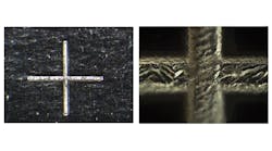
For example, in Figure 1, we see how the technology could be used as a replacement for sinker EDM machines. The picture on the left shows the drilling of a 150-micron hole, ± 10 microns in 200-micron thick steel, with no post processing. The minimal amount of debris and the tight hole tolerance was achieved in 50 percent of the time tIn addition, because the laser marker offers a working XY area, multiple parts can be completed in a single loading operation, as opposed to a one-up loading on the sinker machine (unless an additional investment is made in motion equipment.) This advantage makes the fiber-laser marker ROI (return on investment) even more compelling. The fiber laser can process difficult materials too, such as thin sheet material and foils.
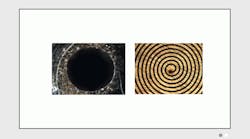
Figure 1 shows the effect of a fiber-laser marker used to drill two 0.006-inch diameter holes. On the left is a 0.01-in. thick precision flow device with a hole-diameter tolerance of ±0.0005 inch. On the right is a spiral with 100-micron wide elements machined into 0.002-in. thick copper foil.
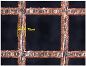
Figure 2 highlights the resolution of the fiber-laser marker with 0.02-in. (0.5-mm) squares machined from 0.002-in. (0.05-mm) thick copper with 0.003-in. (0.075-mm) thick ribs (no post processing.)
Quality control, failure analysis
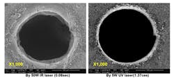
Figure 4 compares the quality of holes drilled with a 20-W single-fiber laser (left) and 5-W 355-nm laser (right) in 0.008-inch stainless steel in the same processing time.
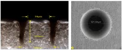
The finesse and machining control that is possible when using the single-mode fiber laser is highlighted in Figure 5. There, the fiber-laser marker was used to machine a 25-micron thick metal foil to a 13-micron depth. The application was to provide a preferential failure point in a component. The channel width was 75 microns and the depth variation over the entire area was ±1 micron. (This equates to taking material that is one-fourth of the width of a human hair and leaving only about one-tenth of a human hair after micromachining.)
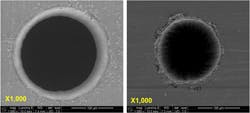
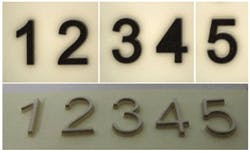
Ceramic is another commonly used material in microelectronics, and a 355-nm laser is typically used for scribing and drilling of ceramic materials. Figures 6 and 7 demonstrate that the fiber-laser marker can be used in ceramics machining. The fiber-laser marker can avoid micro-cracking for a wide variety of features in ceramic materials.
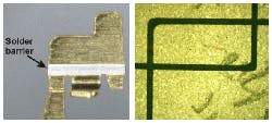
There are many applications that require (or may benefit from) the laser’s ability to selectively remove platings or coatings on metals, ceramics, and even plastics. Fiber-laser machiningtechniques have shown good results in micromachining solder barriers or solder dams, thin-film resistor/capacitor trimming, and active layer removal in battery foils for welding purposes. This selective and tailored layer-removal process is usually impossible during component or part production because masking the area is simply not feasible.
Cost-effective workstation
The laser is extremely useful for selecting the exact resistance value for a circuit. It is excellent when used for resistance or capacitance trimming, as part of a dynamic, iterative removal and measure tuning process in which removal areas may change from one component to the next component.
The single-mode fiber-laser marker can be a cost-effective micromachining workstation for drilling, cutting, scribing, or ablation, for a variety of applications. And, of course, it can mark materials as well! This desktop mini machining center provides the benefits of dual or multi purposing to maximize the return on investment for manufacturers.
It must be noted that, in addition to having the right tool for the job, it is important for the manufacturer to know how to use the tool efficiently and effectively. Miyachi Unitek has developed a number of machining methods that enable the single-mode fiber laser to perform beyond its surface characteristics, while ensuring that the stability of the process is in line with a volume production process.
Geoff Shannon is the laser technology manager for Miyachi Unitek Corp., a manufacturer of equipment and systems for resistance welding, laser welding, laser marking, laser cutting, and hot-bar reflow soldering and bonding. Contact him at 626-303-5676, or [email protected]
